Table of Contents
Introduction
Part 2 of this tutorial can be found HERE
Today we will go step-by-step to create the harware and firmware to load your application from SPI Flash into DDR memory with a MicroBlaze SREC SPI bootloader.
FPGA’s are immensely flexible devices, and although they are capable of running soft core processors this was not the primary motivator behind their development and as such we have to work around some of the limitations they present in this area.
One of the limitations that we will be looking at overcoming is the limited memory available, especially on some of the smaller models for storing application code. Using up all the resources that an FPGA has to offer to implement a soft core is not the best way of gaining access to a microcontroller. You would be better off spending a lot less money on buying a dedicated microcontroller that can do the same thing and that would no doubt be simpler to develop a power distribution network for and subsequent layout on a pcb.
The power of using a soft core on a FPGA comes from using this soft core in conjunction with custom hardware sitting alongside it on the same device. If we cant store the application code on the FPGA we will have to store it somewhere else, the flash memory in this case. Overall the process is quite simple. We use a small srec spi bootloader that is stored using FPGA resoureces, Block or Distributed ram. Its very small. less than 16KB. This bootloader then goes out to the flash and copies our main application over to ram and starts execution from there. This process happens everytime the FPGA is reset or powered on.
Here we will be looking at all the steps required to load an application from flash on a Xilinx FPGA by setting up a MicroBlaze SREC SPI bootloader and then storing the application code on the flash memory of a Arty S7-50 board. This is the same procedure for the Artix boards also.
Setting up the Microblaze
XADC?
The memory interface generator is quite sophisticated in that it uses the temperature data from the XADC to maintain DQS center alignment in the read data window. If you are planning on using the XADC in your design then you can ignore the following steps and simply connect the temperature output from the XADC to the MIG in the bock diagram.
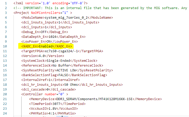
However if you are not planning on using the XADC (It’s not required for the SREC SPI bootloader) then we will have to edit the “mig.prj” file. You can find this file as part of the “Board Files” that you download from the Digilent Github repository. If you are not sure how to add your board files to Vivado then follow this link INSTALL DIGILENT BOARD FILES. I am using the Arty S7-50 here, there are 4 files in the Board folder, “board.xml”, “mig.prj”, “part0_pins.xml” and “preset.xml”. These files contain all the necessary information for Vivado to know exactly what buttons, LEDs, switches and GPIOs are available on the board.
We are only interested in the “mig.prj” file. Creating a memory interface generator IP is quite a complicated process, you need to supply all the pins that the ram is connected to, clock signals, line termination values etc. During this setup process there is an option to select that will cause the MIG to automatically instantiate, connect and use the XADC without any user intervention.
Unfortunately its not possible to amend an already instantiated mig IP and select this option, so instead we will simply amend the mig.prj file so that this will automatically happen when Vivado imports the board files. The mig.prj file is an XML file so changing values inside it is easy, thankfully. We simply need to change the value of the <XADC_En> element in the file from “Disabled” to “Enabled” and save the file, thats it. You can look at the rest of the file if you wish to get an idea of all the information required to setup a MIG. Thankfully the rest of the setup to create the SREC SPI bootloader is not as convoluted as this.
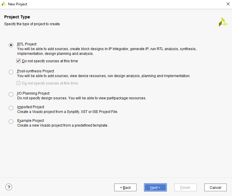
Create new RTL Project
First create a new RTL project – Select “Do not specify sources at this time”.
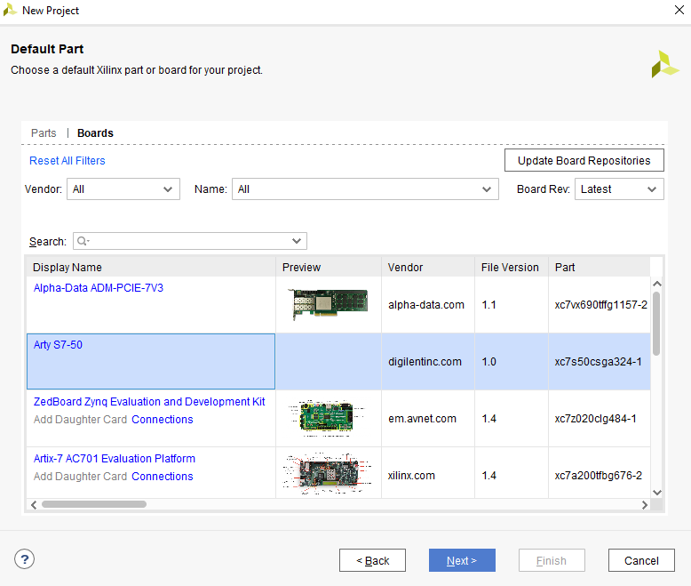
Next select your board that you are using and and hit next, then finish.
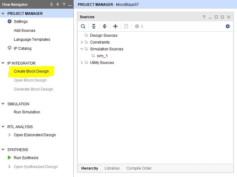
Next start a new IP Integrator block design.
Create the Block Diagram
Select a name for your project, here I chose to call this MicroBlazeS7. Hit OK.

Drag the “System Clock” component from the left onto the Diagram.
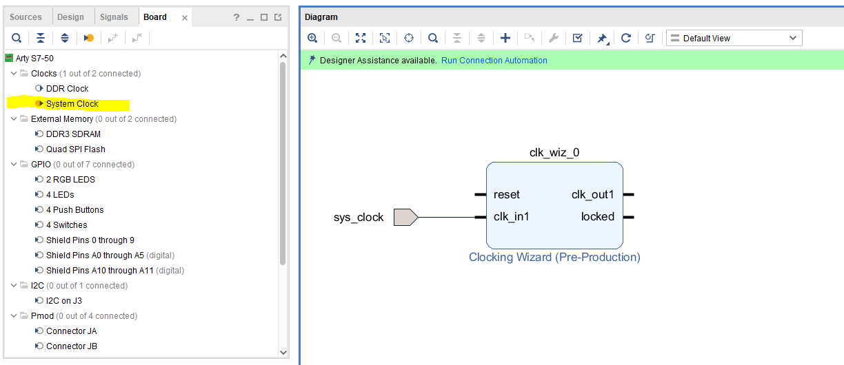
You will now see a clocking wizard block that was added. Double click on the Clocking Wizard to open the customization page. Here, at the bottom of the “Output Clocks” tab, select reset type as “Active Low”. We will leave the default 100MHZ output clock, however you could change this to another value if needed.

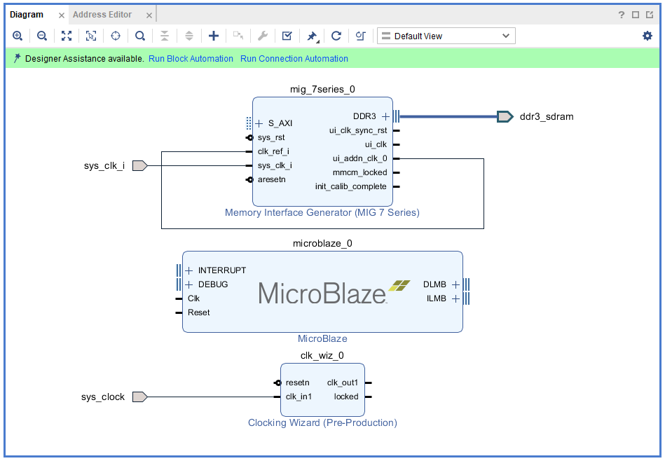
Next drag the DDR3 component onto the block diagram.

You will now see the mig_7series_0 block added. Delete the “clk_ref_i” signal by selecting it and hitting the delete key.

Click and drag the “ui_addn_clk_0” from the right side and connect it to the “clk_ref_i” pin which is now open.

Next add the MicroBlaze soft core by clicking on the “+” symbol on the top toolbar and typing MicroBlaze into the search field. Drag it onto the block diagram.

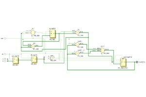
You Should now have a setup looking like this.
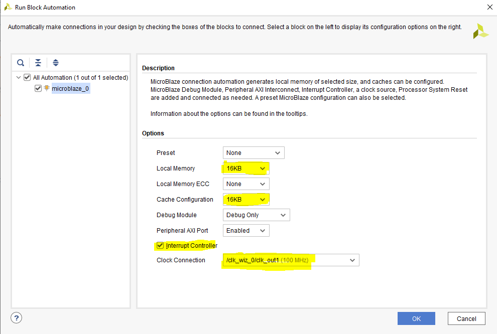
Next click on “Run Block Automation” in the top green bar. Then set 16KB local memory and 16KB Cache. Also tick the box to enable an interrupt controller. We need the 16KB local memory becuase that is where the MicroBlaze SREC SPI bootloader will live. Leave the clock connection on “/clk_wiz_0/clk_out1 (100mhz)”. Then hit OK.
Next, drag the “Quad SPI Flash”, “4 LEDs”, “4 Push Buttons” and the “USB UART” onto the diagram.
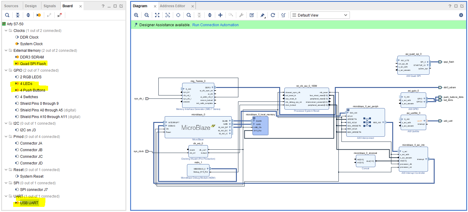
Next, click “Run Connection Automation” in the green bar. After its done click on “Regenerate Layout” in the toolbar to tidy up the layout, then connect the interrupt line from the AXI Uartlite to microblaze_0_xlconcat port 0. Connect the ip2intc_irpt from the AXI Quad SPI to port 1 of microblaze_0_xlconcat as shown in the image below.

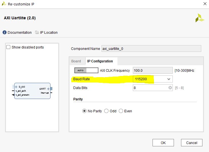
Double click on the “AXI Uartlite” block to open its customization IP. Go to the “IP Configuration tab and set the Baud Rate to 115200.
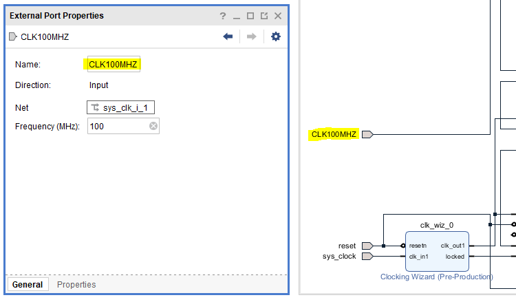
We are almost done now. Finally rename the sys_clk_i to CLK100MHZ by clicking on it and changing the name in the External Port Properties Window.
Right click on the design anywhere and select “Validate Design”, there is also a button for this in the toolbar. It should return saying validation successful.
Add constraints
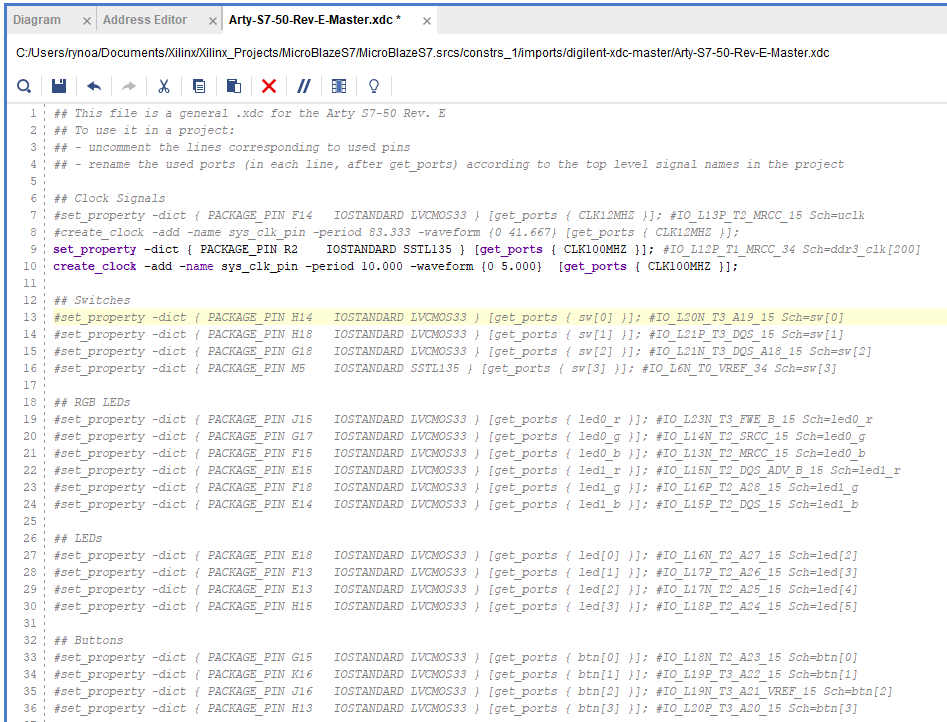
We can now add our constraints file to the project. Digilent have provided us with the constraints files already for all the Arty models here. https://github.com/Digilent/digilent-xdc/
In the sources window click the + icon then select “Add or create constraints. Select the file suitable to your board and check the box that says “Copy constraints files into project” and hit finish.
Open the constraints file and uncomment the properties that sets the constraints for the CLK100MHZ clock signal.
Create wrapper and output products
Right click the project in the Design sources section and select “Create HDL Wrapper”, then select “Let Vivado manage wrapper and auto update” in the dialog box that appears.

You will see a new top level module that contains the board design we created. In my instance it is called “MicroBlazeS7_wrapper”.
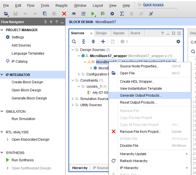
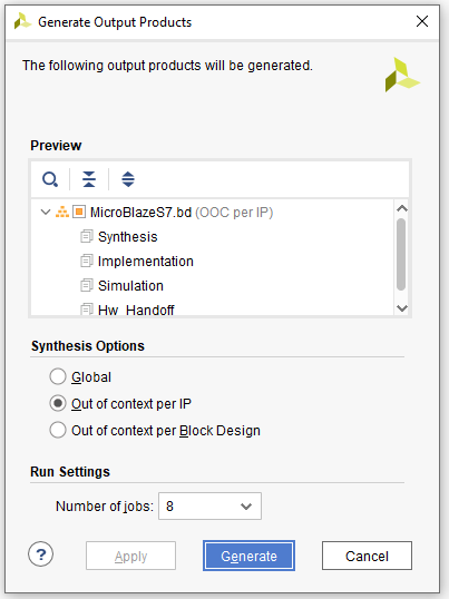
Open up the hierarchy and right click once more on your *.bd board design, the select “Generate Output Products”.
You will see this dialog, leave all the defaults and just click on “Generate”. This will take a while.
Generate the bitstream and export hardware
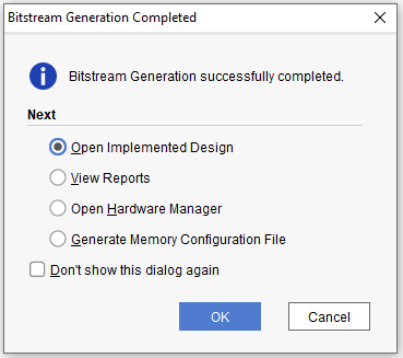
Now click on “Generate Bitstream” and wait for Vivado to do its thing. This also, will take a while so go get a coffee or something. In part 2 we will initialize this bitstream with the spi srec bootloader software.
When its finished with the implementation it will present you with this Dialog Box, select to open the implemented design.
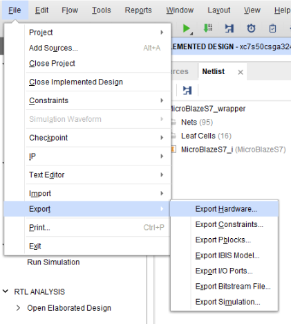
And finally we reach the last step, exporting the hardware so that we can use it in Vitis to complete the software side of this design. This will place a .xsa file with the name you specified into the project directory. We will need this .xsa file later in Vitis.

Firmware with VITIS
In Part 2 we will use Vitis to create the firmware portion of the MicroBlaze SREC SPI bootloader, we will combine the firmware with the bitstream we generated and download this together with a demo application to the Flash. The FPGA will be initialized with the MicroBlaze SREC SPI bootloader, which will then load our demo application from SPI FLASH into DDR memory and then start executing it from there.
