Table of Contents
Introduction
Part 1 of this tutorial can be found HERE
In part 2 we will create a Vitis SREC SPI bootloader software and download this together with a demo application to the Flash. The FPGA will be initialized with the SPI SREC bootloader, which will then load an application from SPI FLASH into DDR memory and then start executing it from there.
Overview
There are four distinct steps to accomplish our goal.
- Create the SREC SPI bootloader software application
- Merge the Bitstream with the bootloader application
- Create the main (DEMO) application
- Program the bitstream and main app to flash
Setting up a new workspace
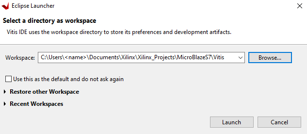
When you first open Vitis it will ask you to select a workspace. You can place this anywhere you wish. I like to keep my projects organized so I placed the Vitis project inside the same folder as the Vivado project.
Create the Vitis SREC SPI Bootloader
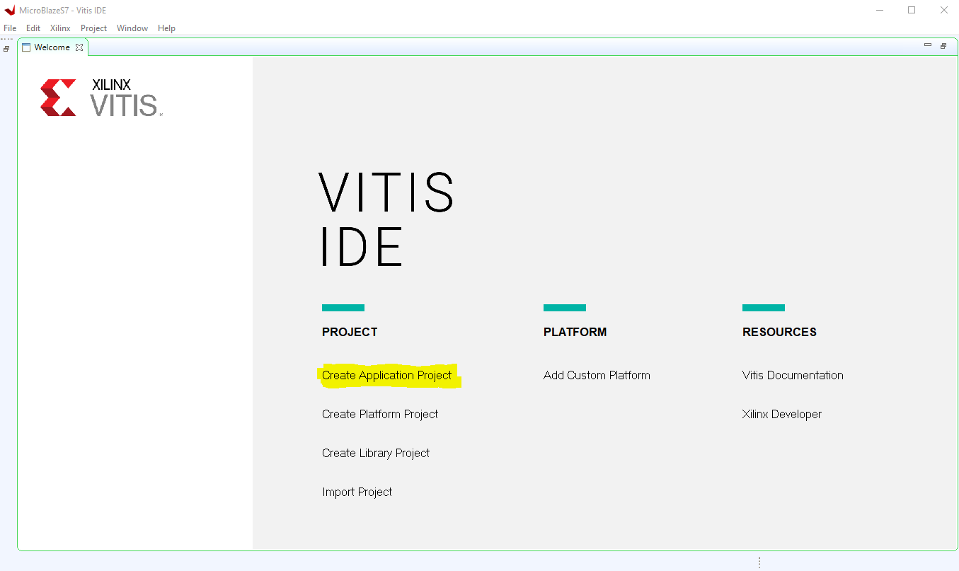
From the Vitis home page select “Create Application Project”
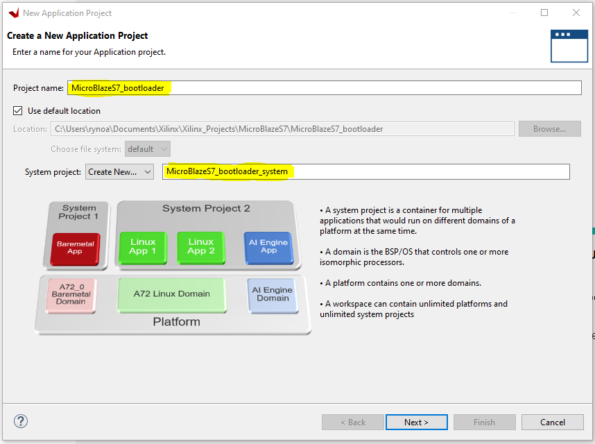
You will be presented with the new application project dialog, here choose a name for your project. You will see that Vitis will also create a new “System Project”, this is normal as a “System Project” is a container for one or more “Application Projects”. Honestly I think they could’ve made this simpler, but there you go.
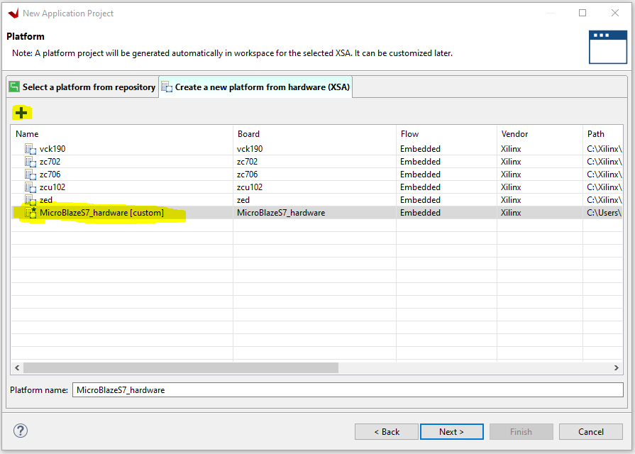
When you hit finish you will be presented with “Platform Project” dialog. Go to the “Create a new platform from harware (XSA)” tab, hit the + icon and add the .xsa file that you exported in Part 1 of this tutorial. With it selected hit next.
Leave the defaults on the next dialog.
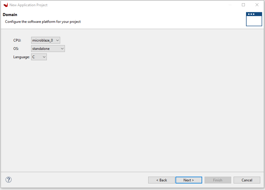
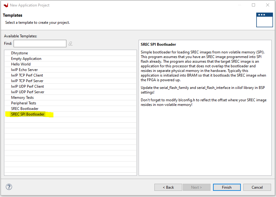
On the final dialog select the “SREC SPI Bootloader” template and click finish.
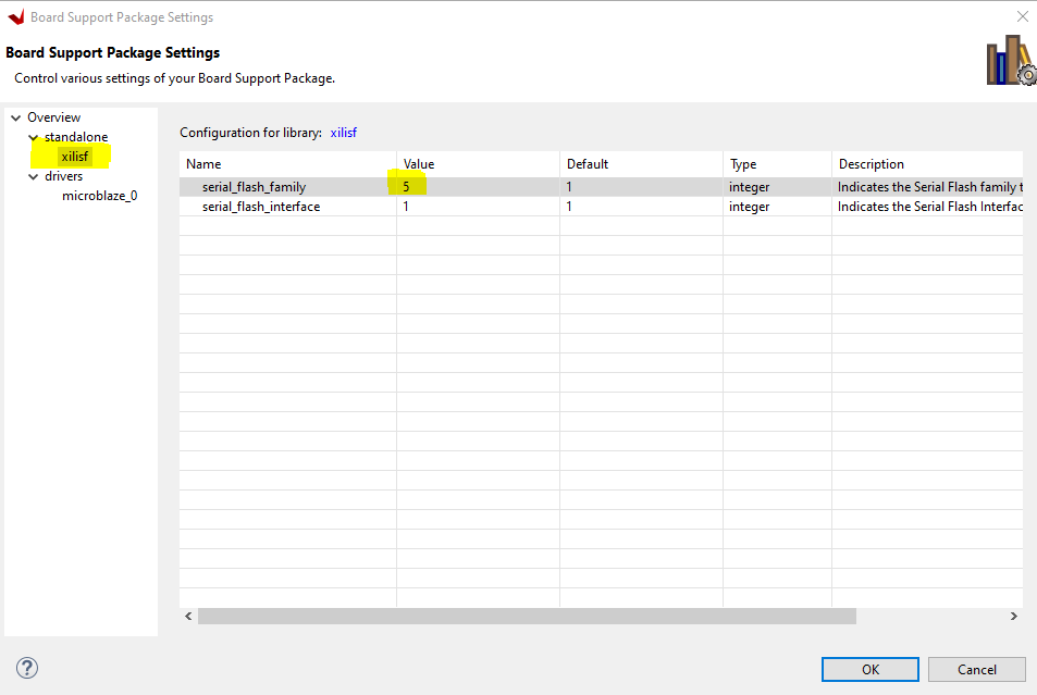
Modify the Board Support Package settings
We now have our base SREC SPI booloader software project started. We want to modify some BSP settings to let Vitis know what Flash we are using and where the offset in the Flash will be where we want to load our main application from. Click on
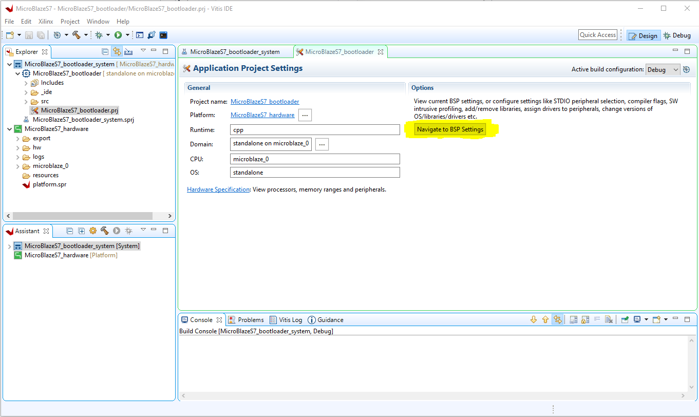
Click on “Modify BSP Settings”.
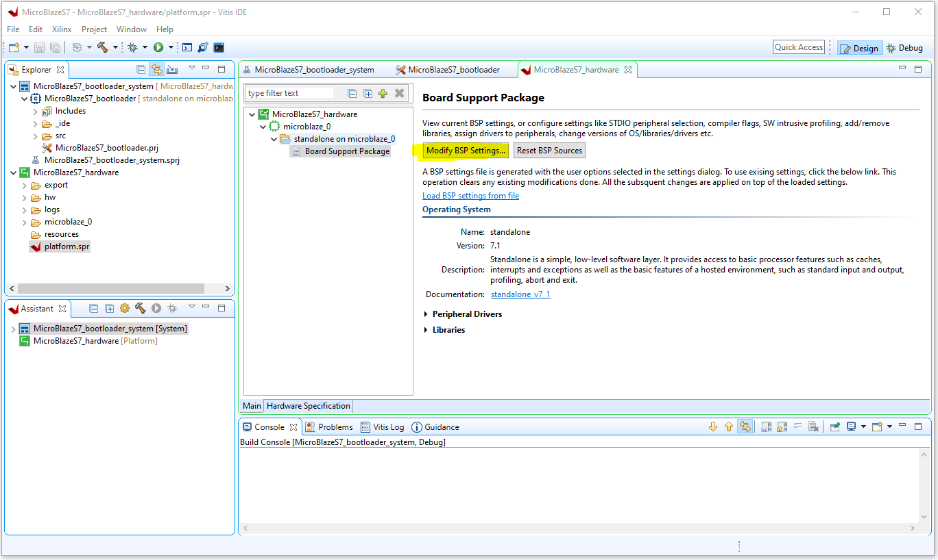
Select Xilisf on the left and set “serial flash family” to 5 as we are using a Micron flash chip. Leave “serial flash interface” on 1 as we are using the SPI interface.
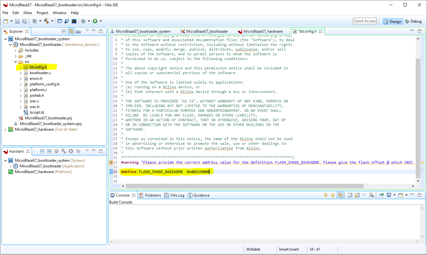
Calculate and set the main app offset
Next we need to tell the srec spi bootloader the offset in the flash memory from where to start copying our main application from.
The physical flash chip on the arty S7-50 is a Micron N25Q128A. Looking at the datasheet it has 4KB erase sectors. 16MB total memory divided by 4KB sectors gives us 4096 total sectors. If we look at our bistream that we created in Part 1, located in <Vivado project directory>\<project name>.runs\impl_1 folder, with a .bit extension we can see that it is 2,192,128 bytes long. Therefore we will need 536 sectors to store it on flash, we can then store our main application from the end of sector 536 onwards, so in other words at an offset of 536 x 4096 = 2,195,456 or 0x00218000 in hex form.
To do this we amend the value of the “FLASH_IMAGE_BASEADDR” macro in the “blconfig.h” file as shown below. This will tell the SREC SPI bootloader software where in flash to find our main app.
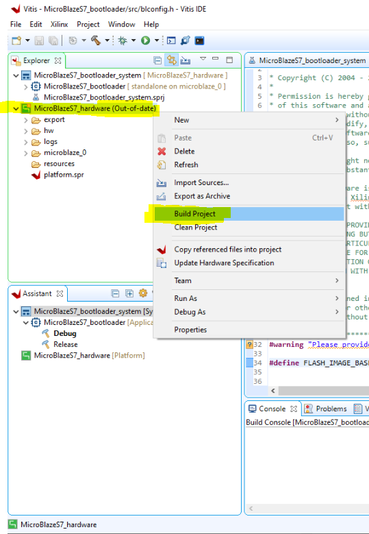
Building the hardware and bootloader app
Lets build the hardware project and our SREC SPI bootloader software that we just created. First build the hardware libraries. Right click on the hardware project in the explorer panel and select “Build Project”. You can also right click on the hardware project in the “Assistant Panel” at the bottom and select build from there.
Right Click on “Release” in the “Assistant” Window under the bootloader app and select build.
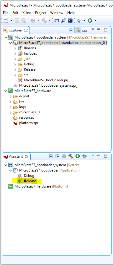
You will see some build errors complaining that the bootloader .bss section does not fit into the 16KB that we allocated for it on Part 1, thankfully this is an easy fix.
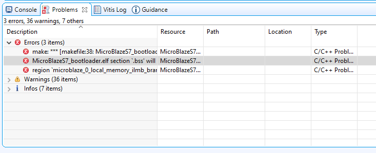
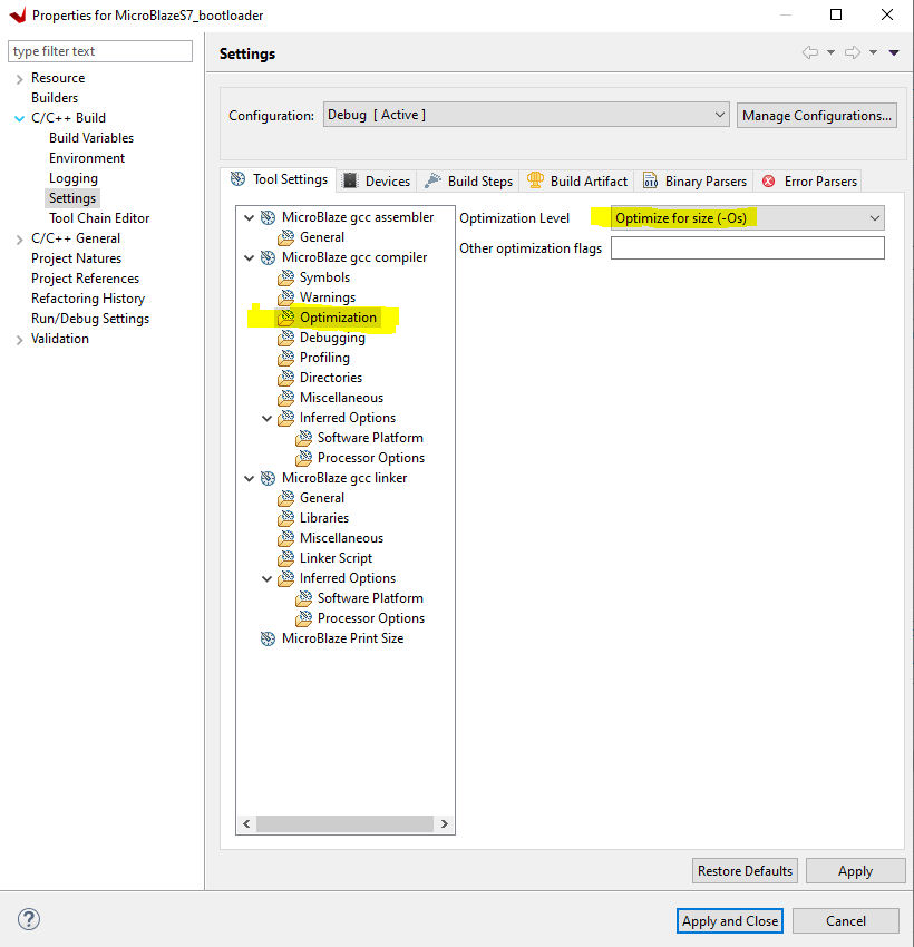
We will have to optimize the build for size so that it will fit, right click your project again and select “C/C++ Build Settings” then select Optimize for size.
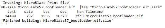
You should get a build with the sizes displayed opposite, it fits neatly inside the 16KB BRAM we allocated for it.
Initialize the bitstream with the bootloader
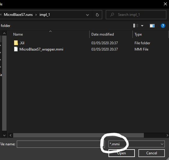
Now we want to combine the bitstream that we generated in Part 1 with this bootloader we just created. We will also need to supply Vitis with the .mmi (Memory Map Info) file that was created when we created the bitstream, its inside the same impl_1 folder. This is an xml file that tells Vitis the layout of the BRAMs where we will store the bootloader, it looks like this.
<?xml version="1.0" encoding="UTF-8"?>
<!-- Product Version: Vivado v2019.2 (64-bit)              -->
<!-- SW Build 2708876 on Wed Nov  6 21:40:23 MST 2019  -->
<!--                                                         -->
<!-- Copyright 1986-2019 Xilinx, Inc. All Rights Reserved.   -->
<!-- Nov  6 2019                                             -->
<!--                                                         -->
<!-- This file is generated by the software with the Tcl write_mem_info command. -->
<!-- Do not edit this file.                                                      -->

<MemInfo Version="1" Minor="6">
  <Processor Endianness="Little" InstPath="MicroBlazeS7_i/microblaze_0">
    <AddressSpace Name="MicroBlazeS7_i_microblaze_0.MicroBlazeS7_i_microblaze_0_local_memory_dlmb_bram_if_cntlr" Begin="0" End="16383">
      <BusBlock>
        <BitLane MemType="RAMB36" Placement="X1Y2">
          <DataWidth MSB="7" LSB="0"/>
          <AddressRange Begin="0" End="4095"/>
          <Parity ON="false" NumBits="0"/>
        </BitLane>
        <BitLane MemType="RAMB36" Placement="X1Y3">
          <DataWidth MSB="15" LSB="8"/>
          <AddressRange Begin="0" End="4095"/>
          <Parity ON="false" NumBits="0"/>
        </BitLane>
        <BitLane MemType="RAMB36" Placement="X1Y4">
          <DataWidth MSB="23" LSB="16"/>
          <AddressRange Begin="0" End="4095"/>
          <Parity ON="false" NumBits="0"/>
        </BitLane>
        <BitLane MemType="RAMB36" Placement="X2Y4">
          <DataWidth MSB="31" LSB="24"/>
          <AddressRange Begin="0" End="4095"/>
          <Parity ON="false" NumBits="0"/>
        </BitLane>
      </BusBlock>
    </AddressSpace>
  </Processor>
  <Config>
    <Option Name="Part" Val="xc7s50csga324-1"/>
  </Config>
  <DRC>
    <Rule Name="RDADDRCHANGE" Val="false"/>
  </DRC>
</MemInfo>
Code language: HTML, XML (xml)
Generate the download.bit file
We now have all the ingredients we need to generate our final bitstream to load onto the flash.
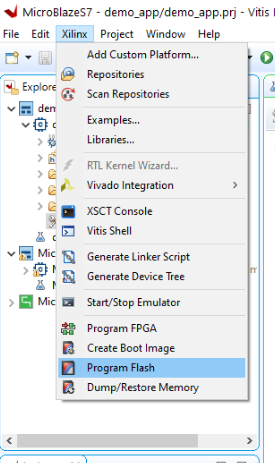
Go to Xilinx->Program FPGA menu.
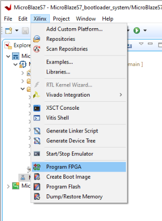
In the dialog box that appears we have to populate a few fields. Add your bitstream that you created in Part 1 (.bit file). Also add your MMI (.mmi file), it defaults to BMM file in the windows explorer window so you will have to change the file type in the bottom right corner. Finally in the “Software Configuration” window select the .elf file we just built. Then hit “Generate”.
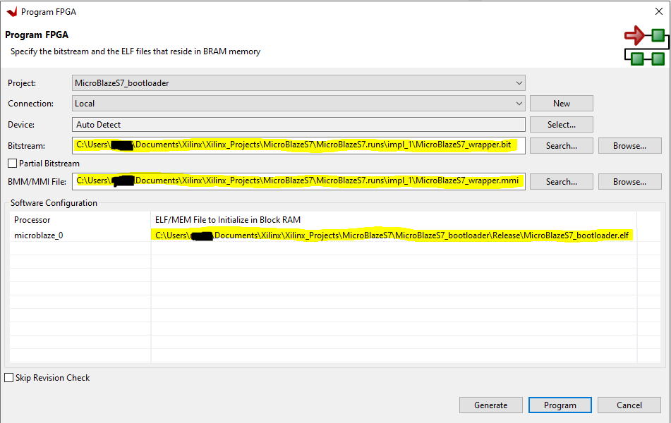
You will now have a file called “download.bit” in the impl_1 folder. This is the Bitstream we created in Part 1 that has now been initialized with the bootloader program we just created. This is part of the FPGA configuration. The FPGA will copy this file from the start of the SPI FLASH when it is turned on or reset, it contains all the configutation details to create our MicroBlaze + the contents of the BRAM (which is our bootloader app). The bootloader will immediatly start executing and copy our main app from address 0x00218000 into DDR and kick off the execution from there.
Create the main (demo) application
Go to File->New Application. Give your demo app a name and hit next.
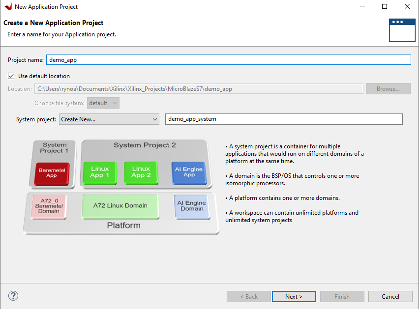
We have already imported our .xsa platform file earlier so its now available on the “Select Platform from Repository” tab.
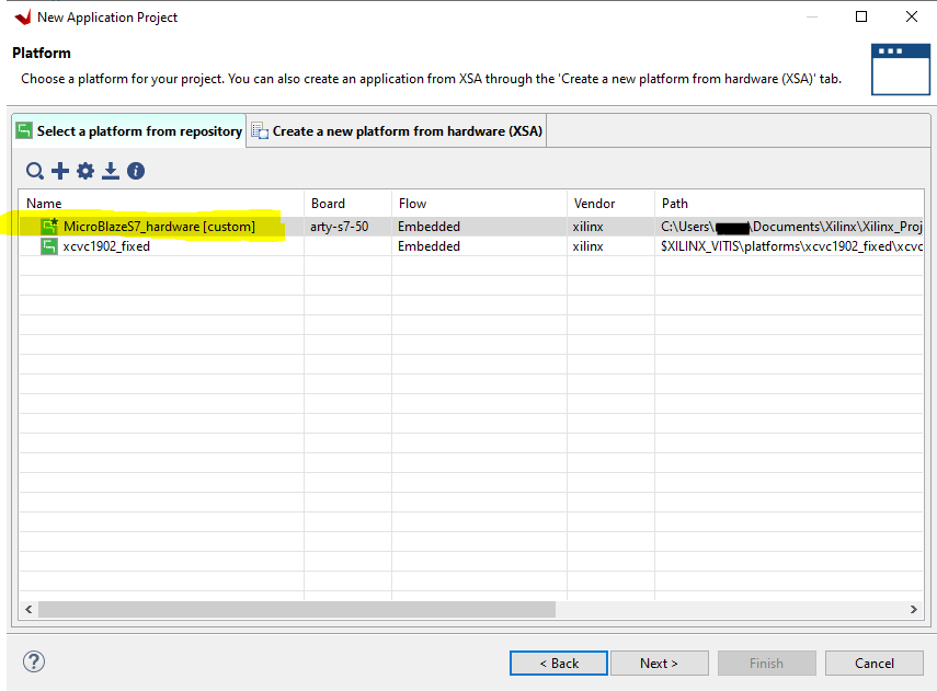
Leave these settings on their default again.
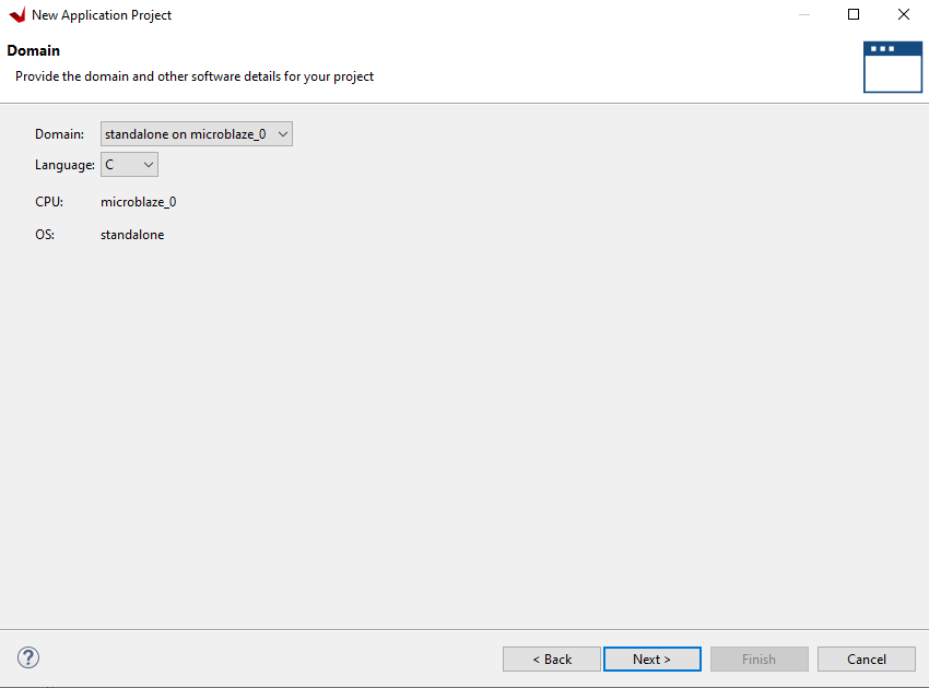
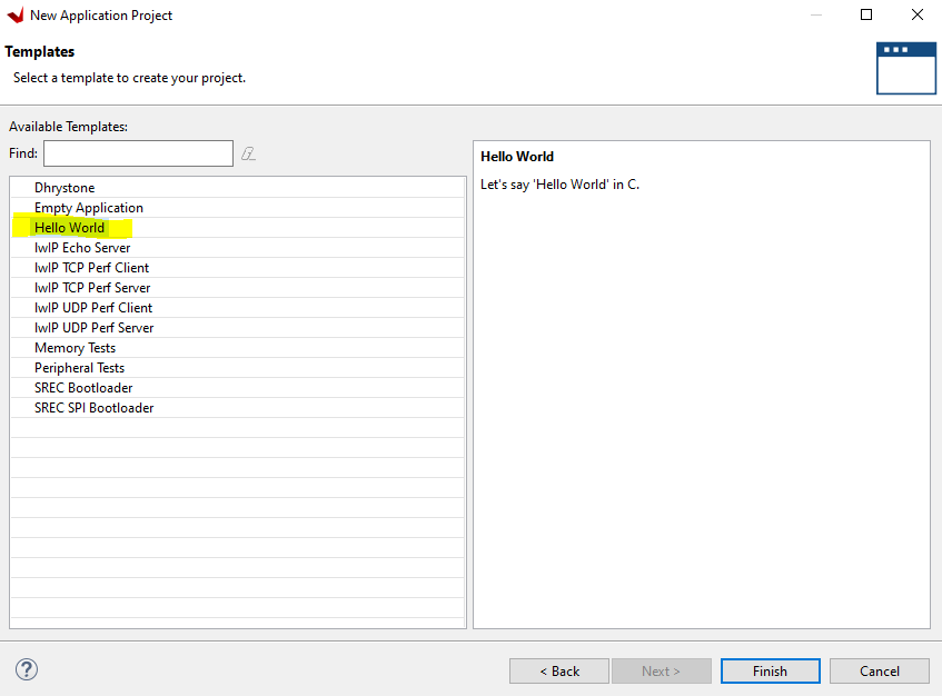
Select the “Hello World” template on the final page and hit finish.
Great! We now have our main app demo, just need to tweak a few things and we’ll be ready to upload everything to the flash.
Review the Linker Script values
Open the the source folder and double-click on the lscript.ld file.
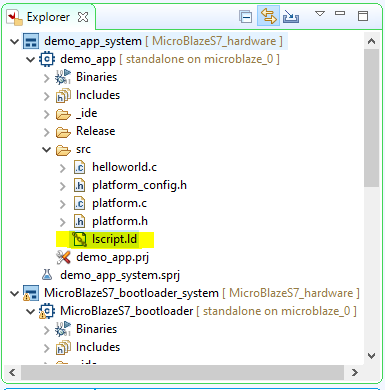
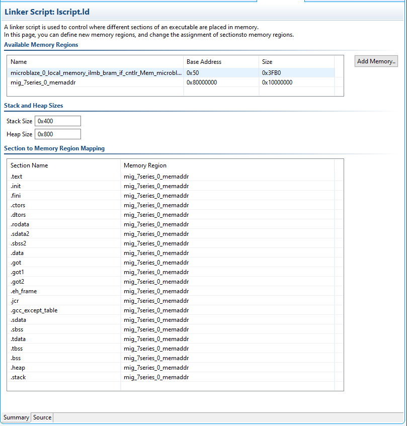
Notice all sections are placed into the DDR memory, which is correct so we dont need to change anything here.
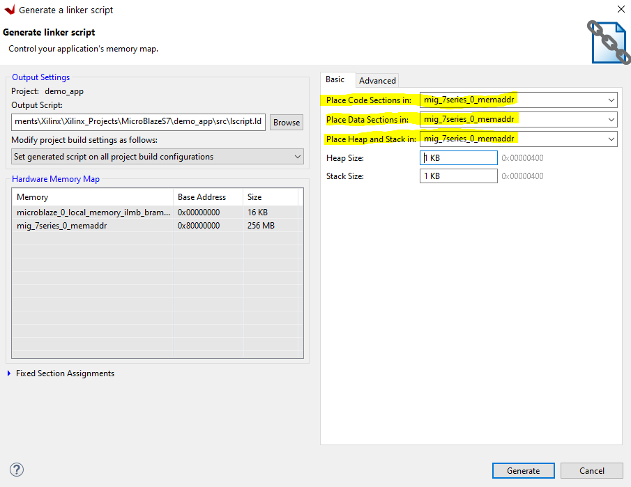
Generate new linker sccript (if necessary)
However, if this was not the case or you wanted to change any of these values there is an easy way to accomplish this.
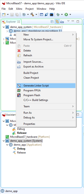
Right Click on the demo application in the explorer and select “Generate Linker Script”
Move the “Code Sections”, “Data Sections” and “Heap and Stack” into the DDR address space (mig_7series_0_memaddr). Leave the default heap and stack size for now. Then hit generate. If it gives you a warning about one already existing just say yes to overwrite it.
Build the Demo App
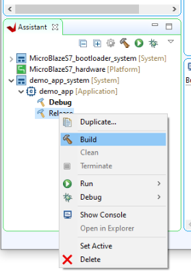
Right click the demo project in the Assistant panel and build it. You can set optimizations if you wish but its not strictly necessary for this demo.
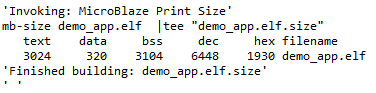
Here is the output from my build.
Writing it all to the flash memory
We will first program the bitsream containing the bootloader to the flash at offset 0x00000000.
We will use the same command to program both the bitstream and the app to the flash. Xilinx->Program Flash.
In the “Program Flash Memory” dialog set the Project as the bootloader we created. The image file is the download.bit in the impl_1 folder that we generated earlier. The offset is 0x0. The flash type (for the Arty S7-50) is mt25ql128-spi-x1_x2_x4. Tick to verify after flash. Hit Program.
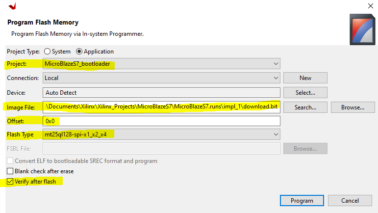
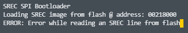
If we run the FPGA now the bootloader will start, look for our demo app at 0x00218000, find nothing and report an error. At least we know everything is working so far.
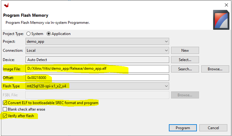
Next we follow the same procedure, but this time we will write the demo app to the flash at the offset we determined earlier (0x00218000). We will additionally tick the box that says “Convert ELF to bootloadable SREC format and program”.
When it all works
This is what you will see when you connect a terminal program to the COM port of the FPGA board. Hoorah! it all works. For any of you wondering what this app below is, its called Terminus, check it out on Github HERE
